- Antenna Point: The point where antenna is connected is called antenna point. It is normally located at the top of the PCB of a mobile phone.
Network Section: The section below antenna point and above power section is called network section.
- Antenna Switch: It is found in the network section. It is made from metal and non-metal. It has 16 points or legs. In some mobile phones, the antenna switch is merged with PFO.
- PFO: Power Frequency Oscillator. It is present beside the antenna switch.
- Network IC: It is below or beside the antenna switch and PFO. In some mobile phones, the Network IC is merged with the CPU. E.g.: Nokia 1200, 1650, 1208, 1209 etc.
Power Section: This section is below the Network Section.
- Power IC: In the Power Section, the IC around which there are several brown-colored capacitors is called Power IC. In some mobile phones there are 2 Power ICs.
- CPU: Central Processing Unit. In the power section, the largest IC is the CPU. In some sets there are 2 CPU.
- Flash IC: This IC is found beside the CPU.
- Logic IC: The IC with 20 legs is the Logic IC.
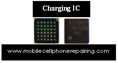
- Charging IC: In the Power Section, the IC beside R22 is the Charging IC.
- Audio IC: The IC parallel to Power IC is the Audio IC.
NOTES:
- UEM (Universal Energy Manager) = Logic IC + Charging IC + Audio IC + Power IC
- PFO (Power Frequency Oscillator) = Antenna Switch + PFO
- Flash IC= RAM + Flash IC


No comments:
Post a Comment